domingo, 27 de junio de 2010

Precise Trace Gas Analysis, Without the Noise

LUIS RINCON EES 18257927
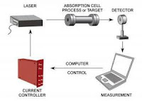


Scientists can analyze atmospheric gas concentrations with laser-based sensors that use systems similar to the one illustrated above. The sensor instrument directs a laser through gas and, based on how much laser light is absorbed by a sample, scientists can determine the specific gases present and their concentrations


Precise Trace Gas Analysis, Without the Noise
ScienceDaily ) — Analyzing trace atmospheric gases can now be considerably more precise with the help of a device that delivers stable and reliable power to the lasers used in gas sensors.


--------------------------------------------------------------------------------

The low-noise current controller was developed at the Department of Energy's Pacific Northwest National Laboratory. The technology was recently licensed to Bozeman, Montana-based Wavelength Electronics Inc. by Battelle, which operates PNNL for DOE.

"Low-noise current controllers open up new ways for us to analyze trace gases," said Matthew Taubman, a PNNL scientist who developed the device. "Now we can evaluate significantly smaller gas concentrations."

Scientists often analyze atmospheric gas concentrations with laser-based sensors. Researchers sample air at sites of interest, such as on the ground near power plants or at high altitudes from airplanes. The sensor instrument then directs a laser through the sample. Based on how much laser light is absorbed by the sample, scientists can determine the specific gases present and their concentrations.

But smaller concentrations of certain gases can be challenging to analyze. One particular problem occurs when "noises," or random fluctuations, exist in a laser's wavelength and line width. Such noise prevents researchers from making precise readings.

PNNL scientists reduced this problem by developing a low-noise current controller. The device reduces the noise on the laser's power source, allowing scientists to detect smaller levels of trace gases. PNNL's controller is the lowest noise controller on the market that was specifically designed for extra-sensitive sensors that use quantum cascade lasers, also called QCLs. Sensors made with QCLs emit light in a wavelength region that many trace gases strongly absorb. QCL-based sensors become even more sensitive when they are powered with low-noise current controllers like PNNL's.

Wavelength Electronics already develops compact current controllers and related components for a variety of semiconductor lasers. Wavelength CEO Mary Johnson also recognized there was a strong potential for her company to make similar QCL-friendly components for Wavelength's customers -- original equipment manufacturers, or OEMs.

That prompted Wavelength to request support through PNNL's Technology Assistance Program, which pairs small businesses looking to overcome specific technology challenges with PNNL scientists. Through the program, Taubman -- the researcher who developed PNNL's low-noise current controller -- compared Wavelength controllers to PNNL low-noise controllers.

At the same time, PNNL and Wavelength brought PNNL's low-noise controllers to one of Wavelength's customers, sensor systems manufacturer Aerodyne Research Inc. of Billerica, Massachusetts. Aerodyne tested the low-noise controllers and learned the devices provided the sensitivity their QCL-based sensors needed. This convinced Johnson that licensing PNNL's controllers would speed up Wavelength's entry into the QCL-based sensor market.

"There's a tremendous need for this technology right now and Wavelength Electronics is pleased to be able to offer it to trace gas researchers and analytical instrument manufacturers," Johnson said.

Wavelength is looking to launch products that incorporate PNNL's low-noise current controller technology by the end of this year. The products will specifically target the QCL market. But other models will be available to work with laser diodes that could be used in microbial detection, skin cancer scanning, DNA sequencing, remote measurements and testing with VCSELs, or vertical cavity surface-emitting lasers, a kind of laser diode.

But Aerodyne didn't want to wait until Wavelength released its new products. Soon after the license went through, Wavelength made the sensor system manufacturer a copy of the low-noise controller for immediate use. Aerodyne is now using these controllers with their most demanding sensor applications, those with continuous-wave QCLs.
http://www.sciencedaily.com/releases/2010/05/100524130844.htm

Researchers Identify the Source of 'Noise' in HIV

LUIS RINCON EES 18257927


Researchers Identify the Source of 'Noise' in HIV
ScienceDaily (Apr. 20, 2010) — New research identifies a molecular mechanism that the human immunodeficiency virus (HIV) appears to utilize for generating random fluctuations called "noise" in its gene expression. The study, published by Cell Press in the April 20th issue of the Biophysical Journal, pinpoints the likely source of HIV gene-expression noise and provides intriguing insight into the role of this noise in driving HIV's fate decision between active replication and latency.


--------------------------------------------------------------------------------

After infecting a human cell, HIV integrates into the genome and typically begins to actively replicate. However, the virus can also enter a long-lived latent state, which remains the greatest barrier to eradicating virus from the patient. Senior study author, Dr. Leor S. Weinberger, a molecular virologist and systems biologist from the Department of Chemistry and Biochemistry at the University of California, San Diego, recently showed that noise in HIV gene-expression critically influences the viral decision to enter either active replication or latency. However, the source of the noise was not clear.

To probe the source of this inherent noise in HIV gene expression, Dr. Abhyudai Singh working in Dr. Weinberger's laboratory exploited a technique from electrical engineering that analyzes how noise changes across different levels of expression. The researchers examined cells carrying a single integrated copy of HIV engineered to produce a quantifiable protein, and measured HIV-1 expression noise at dozens of different viral integration sites which act as distinct genetic environments for viral gene expression.

Surprisingly, the authors find that HIV noise levels are substantially higher than measured in other organisms, and that HIV gene expression occurs in randomly timed bursts. During these expression bursts multiple copies of HIV gene products are produced which leads to the high noise levels in HIV gene expression. The bursting model argues that during active expression HIV cycles between periods of silence and bursting and provides insight into how HIV may be activated by host signaling molecules.

"We know that noise in gene-expression can critically influence HIV's entry to proviral latency. These new results point to transcriptional bursting as a major source of the noise" says Dr. Weinberger. "This finding that transcriptional bursting generates an exceptionally noisy HIV promoter, noisier than almost all other measured promoters, supports the theory that latency may be fundamental to the HIV life cycle and that HIV evolved for probabilistic entry into latency."

Researchers include Abhyudai Singh, University of California, San Diego, La Jolla, CA; Brandon Razooky, University of California, San Diego, La Jolla, CA; Chris D. Cox, University of Tennessee, Knoxville, TN; Michael L. Simpson, Center for Nanophase Materials Sciences, Oak Ridge National Laboratory, Oak Ridge, TN; and Leor S. Weinberger, University of California, San Diego, La Jolla, CA, Whitaker Institute for Biomedical Engineering University of California, San Diego, La Jolla, CA.
http://www.sciencedaily.com/releases/2010/04/100420132828.htm

Molecules As Electric Conductors

LUIS RINCON EES 18257927


Molecules As Electric Conductors
ScienceDaily (July 19, 2009) — Researchers from Graz University of Technology, Humboldt University in Berlin, M.I.T., Montan University in Leoben and Georgia Institute of Technology report an important advance in the understanding of electrical conduction through single molecules.


--------------------------------------------------------------------------------


Minimum size, maximum efficiency: The use of molecules as elements in electronic circuits shows great potential. One of the central challenges up until now has been that most molecules only start to conduct once a large voltage has been applied. An international research team with participation of the Graz University of Technology has shown that molecules containing an odd number of electrons are much more conductive at low bias voltages. These fundamental findings in the highly dynamic research field of nanotechnology open up a diverse array of possible applications: More efficient microchips and components with considerably increased storage densities are conceivable.

One electron instead of two: Most stable molecules have a closed shell configuration with an even number of electrons. Molecules with an odd number of electrons tend to be harder for chemists to synthesize but they conduct much better at low bias voltages. Although using an odd rather than an even number of electrons may seem simple, it is a fundamental realization in the field of nanotechnology – because as a result of this, metal elements in molecular electronic circuits can now be replaced by single molecules. "This brings us a considerable step closer to the ultimate minitiurization of electronic components", explains Egbert Zojer from the Institute for Solid State Physics of the Graz University of Technology.

Molecules instead of metal

The motivation for this basic research is the vision of circuits that only consist of a few molecules. "If it is possible to get molecular components to completely assume the functions of a circuit's various elements, this would open up a wide array of possible applications, the full potential of which will only become apparent over time. In our work we show a path to realizing the highly electrically conductive elements", Zojer excitedly reports the momentous consequences of the discovery.

Specific new perspectives are opened up in the field of molecular electronics, sensor technology or the development of bio-compatible interfaces between inorganic and organic materials: The latter refers to the contact with biological systems such as human cells, for instance, which can be connected to electronic circuits in a bio-compatible fashion via the conductive molecules.

When Noise Becomes the Signal

LUIS RINCON EES 18257927


When Noise Becomes the Signal
ScienceDaily (Apr. 21, 2010) — European researchers have developed a new class of electronics that uses noise -- normally a problem -- as part of the signal. It means better, faster electronics.


"It is a tale, Told by an idiot, full of sound and fury, Signifying nothing," according to Shakespeare's Macbeth. Of course Shakespeare was speaking about the brevity of life, but his words apply equally to noise in a signal.

A signal -- any signal -- inevitably has some noise, a degree of imprecision that carries no information, literally signifying nothing, and even confusing the underlying data. Most of the time engineers work very hard to ensure a high signal to noise ratio -- lots of signal for very little noise.

"That is why in commonly used electronics, the signals are boosted well above noise margins," explains Lukas Worschech, coordinator of the SUBTLE project (http://subtle.fisica.unipg.it/objectives) and a professor at the University of Wurzburg.

That is a fine and worthy goal in most applications, but as devices become smaller, and more complex, the noise becomes a greater and greater problem. It is a bit like dots of ink becoming less sharp as they get smaller, as with impressionist paintings.

"Electronics is based on switches, which can turn on and off signals. The smaller the switches are, the more complex circuits can be realised," notes Worschech.

"However, with increasing miniaturisation of electronic circuits, an increasing fraction of the applied power is converted into nondeterministic signals that add to the ambient noise. It is sometimes referred to as the thermal death of electronics."

The love of limits

It is a problem, and it is setting limits on the miniaturisation, complexity and power of small circuits. Engineers and scientists love limits; it gives them a chance to employ some cunning insight to overcome them.

The scientists and engineers at the SUBTLE project have been very cunning, and their solution is subtle indeed. The project sought to use the noise -- normally a problem -- to boost the signal.

The idea relies on a concept called 'stochastic resonance' (SR), a phenomena in physics first identified in climatology to explain a pronounced variability within the climatic system, where very small changes can lead to profound impacts, such as a mini-ice age.

Stochastic resonance is where a very small variation in a cycle can 'tune in' with other periodical variations to create a massive impact. Its application depends on nonlinear systems, where linear inputs do not equate to linear outputs -- where the sum is greater than the parts.

"This is the SUBTLE solution: do not avoid noise, but exploit noise by SR. This is [made] possible by utilising the feedback action between switches and conducting channels," reveals Worschech. "That is what naturally happens in nanoelectronics. The conductors are very closely spaced to each other. The interaction can even be tailored by the shaping of the conductors."

Forced clarity

Applied to signals, the phenomena opens up the opportunity for engineers to 'force' signal clarity by tuning noise within it. It offers a possible solution to the problem of noise in extremely small components. The idea is not new and was first mooted some years ago, but making it work is an enormous engineering and scientific challenge.

A challenge greeted with gusto by the EU-funded SUBTLE project. The work programme was ambitious; they sought to conceive and create a new class of electronics that uses noise to enhance the signal.

"SUBTLE is a STREP project associated with nanoelectronic devices in which quantum-confined electron channels are so closely spaced to each other that tailored feedback action exists," Worschech notes.

This tailored feedback enhances the signal. The devices employ two, allied, phenomena: back action on the channel gate and noise-induced switching. A channel gate is used to route a signal, and back action is like feedback in an audio system. The subsequent noise can be used to switch the circuit from one channel to another.

Both required very sophisticated circuit design and fabrication and SUBTLE took full advantage of its partners, who are European leaders in the field.

They developed highly novel techniques and pushed the state of the art in a number of domains. They proved selective etching of independent contacts in a double quantum well structure, creating a quantum gate transistor. It is an extremely complex element at nano-scale dimensions and required molecular beam precision to be realised.

These are very sophisticated achievements that enable smaller, cheaper, more power efficient and complex circuits, and they may have application in other fields, too. For example, the SUBTLE team, as part of its work, developed submicron arrays of resonant tunneling diodes that can act as an artificial neuron.

Artificial neurons

These are simple computing, logic gates. Their actions resemble the firing of signals as they are observed between neurons. The SUBTLE team believes that its devices can be thus used in the future to mimic neuron action in artificial networks and to serve as sensors for signals usually hidden under the noise.

This work demonstrates starkly the amazing potential of these new sensors. They can operate at less than millivolts, significantly less that the current state of the art. In combination, they could be used to create neural networks, where actions cascade based in part on the noise of individual spiking neurons. This incredible sensitivity makes the devices an ideal candidate for quantum computing.

And there's more. Typical computers focus on output, the result of a sum: 5 + 2 = 7. Conventional computers discard the input -- the individual transistor states that give us the binary digits. However, the quantum transistors developed by SUBTLE can morph, or reverse, opening the prospect of maintaining the inputs.

"This could be a reversible computer, where you could return to the inputs from the output. It will probably be essential for quantum computing because there will be instances where you need the input," explains Worschech.

These are areas for further research, and the consortium is hoping to set up another project. In the meantime, the project has filed a patent and has been approached by companies that want to build sensors from SUBTLE technology.

"These gates work at such low voltages and with so little noise that they are far ahead of the current state of the art in terms of the sensitivity," Worschech reveals.

The wide variety of applications and the intensity of excitement generated by the SUBTLE project demonstrate the importance of its work. It has led to a new class of electronics and a whole host of potential new solutions to old problems. And all from some very subtle insights.

The SUBTLE project received funding from the FET- Open strand of the EU's Sixth Framework Programme for research.
http://www.sciencedaily.com/releases/2010/04/100422085553.htm

New Material Can Keep Electronics Cool: Few Atomic Layers of Graphene Reveal Unique Thermal Properties

LUIS RINCON EES 18257927


New Material Can Keep Electronics Cool: Few Atomic Layers of Graphene Reveal Unique Thermal Properties
ScienceDaily (May 10, 2010) — Professor Alexander Balandin and a team of UC Riverside researchers, including Chun Ning Lau, an associate professor of physics, have taken another step toward new technology that could keep laptops and other electronic devices from overheating.


Balandin, a professor of electrical engineering in the Bourns College of Engineering, experimentally showed in 2008 that graphene, a recently discovered single-atom-thick carbon crystal, is a strong heat conductor. The problem for practical applications was that it is difficult to produce large, high quality single atomic layers of the material.

Now, in a paper published in Nature Materials, Balandin and co-workers found that multiple layers of graphene, which are easier to make, retain the strong heat conducting properties.

That's also a significant discovery in fundamental physics. Balandin's group, in addition to measurements, explained theoretically how the materials' ability to conduct heat evolves when one goes from conventional three-dimensional bulk materials to two-dimensional atomically-thin films, such as graphene.

The results published in Nature Materials may have important practical applications in removal of dissipated hear from electronic devices.

Heat is an unavoidable by-product when operating electronic devices. Electronic circuits contain many sources of heat, including millions of transistors and interconnecting wiring. In the past, bigger and bigger fans have been used to keep computer chips cool, which improved performance and extended their life span. However, as computers have become faster and gadgets have gotten smaller and more portable the big-fan solution no longer works.

New approaches to managing heat in electronics include incorporating materials with superior thermal properties, such as graphene, into silicon computer chips. In addition, proposed three-dimension electronics, which use vertical integration of computer chips, would depend on heat removal even more, Balandin said.

Silicon, the most common electronic material, has good electronic properties but not so good thermal properties, particularly when structured at the nanometer scale, Balandin said. As Balandin's research shows, graphene has excellent thermal properties in addition to unique electronic characteristics.

"Graphene is one of the hottest materials right now," said Balandin, who is also chair of the Material Sciences and Engineering program. "Everyone is talking about it."

Graphene is not a replacement for silicon, but, instead could be used in conjunction with silicon, Balandin said. At this point, there is no reliable way to synthesize large quantities of graphene. However, progress is being made and it could be possible in a year or two, Balandin said.

Initially, graphene would likely be used in some niche applications such as thermal interface materials for chip packaging or transparent electrodes in photovoltaic solar cells, Balandin said. But, in five years, he said, it could be used with silicon in computer chips, for example as interconnect wiring or heat spreaders. It may also find applications in ultra-fast transistors for radio frequency communications. Low-noise graphene transistors have already been demonstrated in Balandin's lab.

Balandin published the Nature Materials paper with two of his graduate students Suchismita Ghosh, who is now at Intel Corporation, and Samia Subrina, Lau. one of her graduate students, Wenzhong Bao, and Denis L. Nika and Evghenii P. Pokatilov, visting researchers in Balandin's lab who are based at the State University of Moldova.
http://www.sciencedaily.com/releases/2010/05/100510132211.htm

Single-Atom Transistor Discovered

LUIS RINCON EES 18257927


(a) Colored scanning electron microscope image of the measured device. Aluminum top gate is used to induce a two-dimensional electron layer at the silicon-silicon oxide interface below the metallization. The barrier gate is partially below the top gate and depletes the electron layer in the vicinity of the phosphorus donors (the red spheres added to the original image). The barrier gate can also be used to control the conductivity of the device. All the barrier gates in the figure form their own individual transistors. (b) Measured differential conductance through the device at 4 Tesla magnetic field. The red and the yellow spheres illustrate the spin-down and -up states of a donor electron which induce the lines of high conductivity clearly visible in the figure. (Credit: American Chemical Society)

Single-Atom Transistor Discovered
ScienceDaily — Researchers from Helsinki University of Technology (Finland), University of New South Wales (Australia), and University of Melbourne (Australia) have succeeded in building a working transistor, whose active region composes only of a single phosphorus atom in silicon.


--------------------------------------------------------------------------------


The results have just been published in Nano Letters, a journal of the American Chemical Society.

The working principles of the device are based on sequential tunneling of single electrons between the phosphorus atom and the source and drain leads of the transistor. The tunneling can be suppressed or allowed by controlling the voltage on a nearby metal electrode with a width of a few tens of nanometers.

The rapid development of computers, which created the present information society, has been mainly based on the reduction of the size of transistors. Scientists have known for a long time that this development has to slow down critically during the future decades when the even tighter inexpensive packing of transistors would require them to shrink down to the atomic length scales. In the recently developed transistor, all the electric current passes through the same single atom. This allows researchers to study the effects arising in the extreme limit of the transistor size.

"About half a year ago, I and one of the leaders of this research, Prof. Andrew Dzurak, were asked when we expect a single-atom transistor to be fabricated. We looked at each other, smiled, and said that we have already done that," says Dr. Mikko Möttönen. "In fact, our purpose was not to build the tiniest transistor for a classical computer, but a quantum bit which would be the heart of a quantum computer that is being developed worldwide," he continues.

Problems arising when the size of a transistor is shrunk towards the ultimate limit are due to the emergence of so-called quantum mechanical effects. On one hand, these phenomena are expected to challenge the usual transistor operation. On the other hand, they allow classically irrational behavior which can, in principle, be harnessed for conceptually more efficient computing, quantum computing.

The driving force behind the measurements reported now is the idea to utilize the spin degree of freedom of an electron of the phosphorus donor as a quantum bit, a qubit. The researchers were able to observe in their experiments spin up and down states for a single phosphorus donor for the first time. This is a crucial step towards the control of these states, that is, the realization of a qubit.
http://www.sciencedaily.com/releases/2009/12/091206085833.htm

Nanoelectronic Transistor Combined With Biological Machine Could Lead To Better Electronics

LUIS RINCON EES 18257927

Nanoelectronic Transistor Combined With Biological Machine Could Lead To Better Electronics


Nanoelectronic Transistor Combined With Biological Machine Could Lead To Better Electronics
ScienceDaily (Sep. 7, 2009) — If artificial devices could be combined with biological machines, laptops and other electronic devices could get a boost in operating efficiency.

An artist's representation of a nanobioelectronic device incorporating alamethycin biological pore. In the core of the device is a silicon nanowire (grey), covered with a lipid bilayer (blue). The bilayer incorporates bundles of alamethicin molecules (purple) that form pore channels in the membrane. Transport of protons though these pore channels changes the current through the nanowire. (Credit: Image by Scott Dougherty, LLNL)
--------------------------------------------------------------------------------


Lawrence Livermore National Laboratory researchers have devised a versatile hybrid platform that uses lipid-coated nanowires to build prototype bionanoelectronic devices.

Mingling biological components in electronic circuits could enhance biosensing and diagnostic tools, advance neural prosthetics such as cochlear implants, and could even increase the efficiency of future computers.

While modern communication devices rely on electric fields and currents to carry the flow of information, biological systems are much more complex. They use an arsenal of membrane receptors, channels and pumps to control signal transduction that is unmatched by even the most powerful computers. For example, conversion of sound waves into nerve impulses is a very complicated process, yet the human ear has no trouble performing it.

"Electronic circuits that use these complex biological components could become much more efficient," said Aleksandr Noy, the LLNL lead scientist on the project.

While earlier research has attempted to integrate biological systems with microelectronics, none have gotten to the point of seamless material-level incorporation.

"But with the creation of even smaller nanomaterials that are comparable to the size of biological molecules, we can integrate the systems at an even more localized level," Noy said.

To create the bionanoelectronic platform the LLNL team turned to lipid membranes, which are ubiquitous in biological cells. These membranes form a stable, self-healing,and virtually impenetrable barrier to ions and small molecules.

"That's not to mention that these lipid membranes also can house an unlimited number of protein machines that perform a large number of critical recognition, transport and signal transduction functions in the cell," said Nipun Misra, a UC Berkeley graduate student and a co-author on the paper.

Julio Martinez, a UC Davis graduate student and another co-author added: "Besides some preliminary work, using lipid membranes in nanoelectronic devices remains virtually untapped."

The researchers incorporated lipid bilayer membranes into silicon nanowire transistors by covering the nanowire with a continuous lipid bilayer shell that forms a barrier between the nanowire surface and solution species.

"This 'shielded wire' configuration allows us to use membrane pores as the only pathway for the ions to reach the nanowire," Noy said. "This is how we can use the nanowire device to monitor specific transport and also to control the membrane protein."

The team showed that by changing the gate voltage of the device, they can open and close the membrane pore electronically.

The research appears Aug. 10 in the online version of the Proceedings of the National Academy of Sciences.

Photography: Blur's Noise And Distortion Reversed

LUIS RINCON EES 18257927


Photography: Blur's Noise And Distortion Reversed
ScienceDaily (July 9, 2009) — Errant pixels and blurry regions in a photo, whether digital or scanned, are the bane of photographers everywhere. Moreover, in vision processing research degraded photos are common and require restoration to a high-quality undegraded state. Research published in the International Journal of Signal and Imaging Systems Engineering could provide new insights.


--------------------------------------------------------------------------------


There are countless examples of image editors and photo cleanup software that have built-in tools designed to remove noise and sharpen up edges. Some of these are very powerful others less so. Any "cleanup" process that works by changing individual pixels leads to overall degradation of the image and loss of information. However, a delicate touch with the most subtle tools can produce acceptable quality results.

Now, S. Uma of the Department of Electronics and Communication Engineering, at Coimbatore Institute of Technology, and S. Annadurai of the Government College of Technology, Coimbatore, India, have turned to neural networks to help them clean up their image. The approach could significantly reduce information loss while reversing blurring caused by lens aberrations and faults and reducing noise that distorts the appearance of an image. The team suggests that distortions in an image due to atmospheric disturbances between camera and distant subjects could be unraveled and a photo taken on a hot, hazy day made acceptable.

The researchers point out that earlier attempts at this kind of inverse filtering of an image rely on the image having a high signal-to-noise (SNR) ratio. Other approaches require huge amounts of computing power and are generally untenable. This is especially true in the fledgling field of artificial vision, whether robotic or prosthetic. However, some success with neural networks has been achieved.

Now, Uma and Annadurai have developed a modified recurrent Hopfield neural network that builds and extends the work of others to allow them to quickly process an image reducing distortion, noise and blurring. The team has tested their approach on square grayscale images just 256 pixels across. They were able to reverse severe blurring and noise deliberately added to the original photographic sample to much more acceptable levels in a short time using limited computing resources than was possible with previous neural network approaches or any other inverse filtering techniques.

An analysis of the before and after quality shows that quality is improved by between 39% and 67% using the team's approach and results take half the time of other methods that produce lesser improvements. The success bodes well for image processing, in various fields including vision research, art, homeland security, and science.

http://www.sciencedaily.com/releases/2009/07/090708094827.htm

Electrosmog on the circuit board

LUIS RINCON EES 18257927


Electrosmog On The Circuit Board
http://www.sciencedaily.com/releases/2009/04/090406102630.htm
ScienceDaily (Apr. 9, 2009) — The smaller the components in electronic circuits, the more interference-prone they are. If the components are too densely packed, they can interfere with one another. A near-field scanner can accurately detect weak fields and help to protect bank cards against fraud.


--------------------------------------------------------------------------------


Their miniature size is their strength – and also their weakness. Be it in cell phones, cars or computers, electronic components are getting smaller and smaller and increasingly powerful. The smaller they are, the faster they can switch and the less energy they need for each switching operation. However, as energy requirements shrink, so do signal-to-noise ratios. "Circuits are becoming more and more susceptible with each generation," explains Thomas Mager of the Fraunhofer Research Institution for Electronic Nano Systems ENAS in Paderborn.

"Only a few years ago, it still took several volts to destabilize processors. Today, a few hundred millivolts are sometimes enough to disrupt millions of transistors." This means that designers of electronic circuits need to give greater consideration to electromagnetic compatibility. It is no longer just a question of protecting complete electronic packages such as cell phones or MP3 players against external influences, or shielding the environment against their electromagnetic emissions, but is also about how each individual component on the circuit board behaves.

In a collaborative project carried out with Continental and Infineon Technologies, the Fraunhofer ENAS has developed a measuring system that can locate even the weakest electrical and magnetic fields to an accuracy of a few hundredths of a millimeter. Where are there areas of conspicuously high electromagnetic radiation? How do the components influence one another? The near-field scanner can scan not only individual chips and processors but also complete laptops, cell phones or aircraft control units, and can reveal which types of field the test object is radiating.

"We are also working with our French project partner CEA-Leti on a function that applies targeted electromagnetic fields to the test object. In this way, we can test for areas that respond sensitively to external fields," says Mager. This makes the system particularly interesting for developers of smart cards. Fraudsters elicit confidential information from bank cards by bombarding them with pulses of laser light, electrical current or voltage. The resulting field patterns can reveal details about the chip card, such as its PIN number. The near-field scanner provides time- and space-resolved images of the radiated fields of the card, allowing their weak points to be identified and helping card developers to better protect their products against fraud.

Discovery Promises To Improve Semiconductor-Based Sensors


Publicado por Luis Rincon CI 18257927 EES


Illustration of a Coulomb glass system: Electrons (red) in a random landscape, interacting with each other (yellow-orange lines). Noise of the resistance of the system is created by collective "hopping" of the electrons (green arrow). (Credit: Image courtesy of DOE/Argonne National Laboratory)

Discovery Promises To Improve Semiconductor-Based Sensors
ScienceDaily (May 10, 2007) — More sensitive sensors and detectors based on semiconductor electronics could result from new findings by researchers from the United States, Norway and Russia.

http://www.sciencedaily.com/releases/2007/05/070509161026.htm

--------------------------------------------------------------------------------


Their research has yielded a decisive step in identifying the origin of the universal "one-over-f" (1/f) noise phenomenon; "f" stands for "frequency."

"One-over-f noise appears almost everywhere, from electronic devices and fatigue in materials to traffic on roads, the distribution of stars in galaxies, and DNA sequences," said Valerii Vinokour or Argonne's Materials Science Division. "Finding the common origin of one-over-f noise in its many forms is one of the grand challenges of materials physics. Our theory establishes the origin and lower limit to one-over-f noise in semiconductor electronics, helping to optimize detectors for commercial application."

Noise is a fluctuation in time, a deviation from the average. Humans and other animals carry a common example in their heartbeats, where 1/f noise can be detected as a deviation from normal pulse. In nanomaterials, such as the tiny circuits in semiconductor electronics, the noise generated by the random motion of a single electron can be devastating, since there are so few electrons in the system.

Vinokur and his team showed that the 1/f noise in doped semiconductors, the platform for all modern electronics, originates in the random distribution of impurities and the mutual interaction of the many electrons surrounding them. These two ingredients — randomness and interaction — trap electrons in the Coulomb glass, a state like window glass where electrons move by hopping from one random location to another. 1/f noise arises from the electrons; hopping motion. After discovering the theoretical connection between 1/f noise and formation of the Coulomb glass, Vinokur and his collaborators confirmed it with large-scale computer simulations: suppression of the interactions was found to remove the Coulomb glass behavior and 1/f noise.

"Our results," Vinokour said, "establish that one-over-f noise is a generic property of Coulomb glasses and, moreover, of a wide class of random interacting systems and phenomena ranging from mechanical properties of real materials and electric properties of electronic devices to fluctuations in the traffic of computer networks and the Internet."

These research findings were published in the May 11 issue of Physical Review Letters.

Collaborators on this research were Vinokur and Andreas Glatz, at Argonne, Y.M. Galperin from University of Oslo, Oslo, Norway, and A.F. Ioffe of the Physico-Technical Institute of the Russian Academy of Sciences, St. Petersburg, Russia.

Nano-Chips To Power Computers, Phones Of The Future

Luis Rincon EES 18257927

Nano-Chips To Power Computers, Phones Of The Future

Nano-Chips To Power Computers, Phones Of The Future
ScienceDaily (July 8, 2006) — British scientists are playing a key role in the drive to make electronic gadgets smaller, smarter and even more powerful. Researchers from five universities are designing a new generation of 'nano-electronic' circuits (chips) that will power the computers and mobile phones of the future. The circuits may also make possible entirely new forms of electronic device that could benefit a range of sectors, including entertainment, communications and medicine.


--------------------------------------------------------------------------------


The quest for new circuits has been prompted by the relentless advance of technology, which is now proving to be a real headache for the microelectronics industry. The microscopic transistors which are the cogs and wheels of all electronic devices are becoming even smaller and designers must now devise electronic circuits that are compatible with them.

Teams at the Universities of Edinburgh, Glasgow, Manchester, Southampton and York are striving to create nanoscale circuits, using transistors that are 80,000 times smaller than a hair's breadth. Because the circuits in today's ipods and PCs will not work with nano-transistors, this research – which is funded by the Engineering and Physical Sciences Research Council – is vital to prevent the industry from grinding to a halt.

In the next decade, transistors will not only be ten times smaller – they will also behave very differently. Two of todays transistors, identical in shape and size, will behave in more or less the same way. That, however, will not be the case at nanoscale.

The next generation of transistors will, in the jargon of chip design, be 'unmatched'– despite being apparently identical. They will also be extremely 'noisy', adding a strong random signal of their own (known as device noise) to whatever signal they are dealing with.

"The circuits we currently use cannot cope with this form of mismatch and randomness," says Professor Alan Murray, of the University of Edinburgh. "They will require at least re-design - possibly even complete replacement - with circuits that have not yet been invented. We can't wait for silicon technology to create viable, production-line nanoscale transistors. It will then be too late to start looking for ways to use them. We must start now."

This new project will allow circuits to be designed that can cope with, or even make use of, the unavoidable bad behaviour of nanoscale transistors. It will use e-Science – which draws on shared data and massive computing power – to bring together computer simulations of transistors that do not yet exist and simulations of circuits that use them.

Principal investigator, Professor Asen Asenov, of the University of Glasgow, is looking forward to the challenge: "This project brings together leading semiconductor device, circuit and system experts from academia and industry and e-scientists with strong Grid expertise. Only by working in close collaboration, and adequately connected and resourced by e-Science and Grid technology, can we understand and tackle the design complexity of nano-CMOS electronics, securing a competitive advantage for the UK electronics industry."

Professor Richard Sinnott, of the National e-Science Centre at the University of Glasgow, who will lead the e-Science development activity, is also eagerly anticipating the project: "Through close collaboration with our partners, we expect to revolutionise the way in which the disparate teams involved in electronics design process work. Our Grid efforts will be on four key areas: workflows, security, data management and resource management, each targeted to the real needs of the scientists we are to support."
http://www.sciencedaily.com/releases/2006/07/060708082927.htm

Discovery Promises To Improve Semiconductor-Based Sensors

Publicado por Luis Rincon CI 18257927 EES


Illustration of a Coulomb glass system: Electrons (red) in a random landscape, interacting with each other (yellow-orange lines). Noise of the resistance of the system is created by collective "hopping" of the electrons (green arrow). (Credit: Image courtesy of DOE/Argonne National Laboratory)

Discovery Promises To Improve Semiconductor-Based Sensors
ScienceDaily (May 10, 2007) — More sensitive sensors and detectors based on semiconductor electronics could result from new findings by researchers from the United States, Norway and Russia.

http://www.sciencedaily.com/releases/2007/05/070509161026.htm

--------------------------------------------------------------------------------


Their research has yielded a decisive step in identifying the origin of the universal "one-over-f" (1/f) noise phenomenon; "f" stands for "frequency."

"One-over-f noise appears almost everywhere, from electronic devices and fatigue in materials to traffic on roads, the distribution of stars in galaxies, and DNA sequences," said Valerii Vinokour or Argonne's Materials Science Division. "Finding the common origin of one-over-f noise in its many forms is one of the grand challenges of materials physics. Our theory establishes the origin and lower limit to one-over-f noise in semiconductor electronics, helping to optimize detectors for commercial application."

Noise is a fluctuation in time, a deviation from the average. Humans and other animals carry a common example in their heartbeats, where 1/f noise can be detected as a deviation from normal pulse. In nanomaterials, such as the tiny circuits in semiconductor electronics, the noise generated by the random motion of a single electron can be devastating, since there are so few electrons in the system.

Vinokur and his team showed that the 1/f noise in doped semiconductors, the platform for all modern electronics, originates in the random distribution of impurities and the mutual interaction of the many electrons surrounding them. These two ingredients — randomness and interaction — trap electrons in the Coulomb glass, a state like window glass where electrons move by hopping from one random location to another. 1/f noise arises from the electrons; hopping motion. After discovering the theoretical connection between 1/f noise and formation of the Coulomb glass, Vinokur and his collaborators confirmed it with large-scale computer simulations: suppression of the interactions was found to remove the Coulomb glass behavior and 1/f noise.

"Our results," Vinokour said, "establish that one-over-f noise is a generic property of Coulomb glasses and, moreover, of a wide class of random interacting systems and phenomena ranging from mechanical properties of real materials and electric properties of electronic devices to fluctuations in the traffic of computer networks and the Internet."

These research findings were published in the May 11 issue of Physical Review Letters.

Collaborators on this research were Vinokur and Andreas Glatz, at Argonne, Y.M. Galperin from University of Oslo, Oslo, Norway, and A.F. Ioffe of the Physico-Technical Institute of the Russian Academy of Sciences, St. Petersburg, Russia.